The wide bandgap semiconductors with direct bandgap can emit light as most people learned when Nobel prize was awarded for the LEDs in 2014. The researchers already had worked for about two decades on those materials like GaN, AlN and InN. The latter one, (indium nitride) was a little bit peculiar among them with its forbidden bandgap of 0.7 eV, i.e. not very wide. However, the above three materials can be grown easily in a ternary form and InN played a crucial role in the preparation of light emitting diodes (LED) and lasers in the form of InxGa1-xN. The bandgap and the wavelength of the emitted light can be tuned with the indium content. The exploration of 2D materials together with valuable theoretical papers predicted that the nitrides will possess also novel properties. Researchers supposed that the bandgap of the bilayer InN will be widen and can be used as a light emitting layer in the visible range.
The work which resulted in a bilayer of indium nitride formed in the closed space of hydrogenated epitaxial graphene on SiC was carried out in a FLAG ERA project called GRIFONE in a cooperation of Sweden, Italy and Hungary. The coordinator of the project with overall conceptualization and course of research is Anelia Kakanakova (Linköping University, Sweden), while partners are Filippo Giannazzo (CNR Catania, Italy) and Béla Pécz (ELKH EK MFA). The project aimed the development of a general platform which provides the possibility to grow 2D semiconductors by (Metalorganic Vapour Deposition). Successful examples are 2D AlN (published earlier in Nanoscale) and the subject of this news, indium nitride. The successful outcome of the research on 2D InN was led by Béla Pécz.
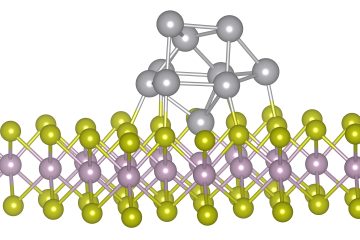
The buffer layer of epitaxial graphene on SiC turns to an additional graphene layer, weekly bond to the substrate, therefore we can let metal atoms into the space of graphene-SiC by intercalation. That was used in the present experiments as well providing indium atoms and nitrogen from ammonia by MOCVD (by AK, Linköping University, Sweden). The results clearly show that the formed layer is successfully stabilized.
The whole surface of the sample was investigated by conductive AFM (by F.G, CNR Catania, Italy), which showed that more than 90% of the sample surface is covered by InN (below the graphene). Occasionally thicker inclusion of InN (5-7 layer thick) were also traced still under the graphene.
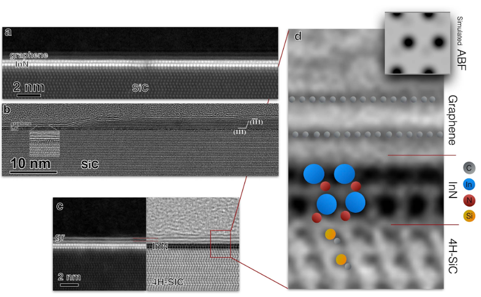
The image a) in the next figure shows the bilayer InN in the aberration corrected THEMIS 200 microscope of MFA (HAADF image in STEM mode). The intensity is proportional with square of the atomic number and one can see clearly the two rows of the indium atoms. Image b) shows the rearly observed 3D InN, which actually shows cubic layer sequence. Figure c) shows an (annular bright field) Image which provides the possibility to observe the light elements as well and indeed on the right side one can observe the nitrogen bond to indium as well as the carbon in SiC.
The final proof for the chemical composition of the bilayer was provided by EELS (Electron Energy Loss Spectroscopy) carried out by Giuseppe Nicotra CNR-IMM Beyond Nano laboratory. The results clearly showed the fine structure of Nitrogen K edge and that the layer is oxygen free.
The importance of the new findings was enhanced by the work of Antal Koós (ELKH EK MFA) when he took I-V characteristics place by place on the sample by STS (Scanning Tunnelling Spectroscopy) . The results showed a bandgap of 2±0.1 eV instead of the 0.7 eV for the bulk case. With this synthesis the 2D InN took its place among the real wide bandgap semiconductors.
The full paper is available here: https://onlinelibrary.wiley.com/doi/full/10.1002/adma.202006660