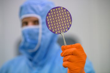
The “Forefront” research group at the Centre for Energy Research of the Eötvös Loránd Research Network, led by Levente Tapasztó, has realized for the first time graphene plasmons in the visible frequency range, using nanoengineered graphene structures. The results have been published in the prestigious Nature Nanotechnology journal. As a first application of visible-frequency graphene plasmons, the researchers were able to demonstrate the optical detection of specific molecules with three orders of magnitude higher sensitivity than previously achieved with graphene. Due to its practical significance in high sensitivity optical detection, the researchers have also applied for patenting the nanocorrugated graphene sensors working with visible light.
Light and matter can interact in various ways. An intriguing type of light-matter interaction occurs when incoming light induces a collective oscillation of the electron system, giving rise to a new type of quasi-particles, named plasmons (or more precisely: surface plasmon polaritons). Only specific, so-called plasmonically active materials allow such type of light-matter interaction. On the surface of plasmonic materials, the rapidly changing electric field of the incoming light, induces a collective oscillation of the electron system, with the same frequency, but significantly reduced wavelength, compared to the freely propagating light. This corresponds to squeezing light into smaller mode volumes that in turn gives rise to huge local electric fields, and light intensities.
The researchers lead by Levente Tapasztó at the Nanostructures Department of the Institute of Technical Physics and Materials Science have investigated how to create plasmon of frequencies in the visible optical range in graphene. Graphene is a single atom thick crystal consisting of a honeycomb lattice of carbon atoms, characterized by a unique electronic structure. The charge carriers of graphene are of zero effective mass. It is an intriguing question, whether light can couple to such a unique electron system, and if so, what the properties of the resulting graphene plasmons will be?
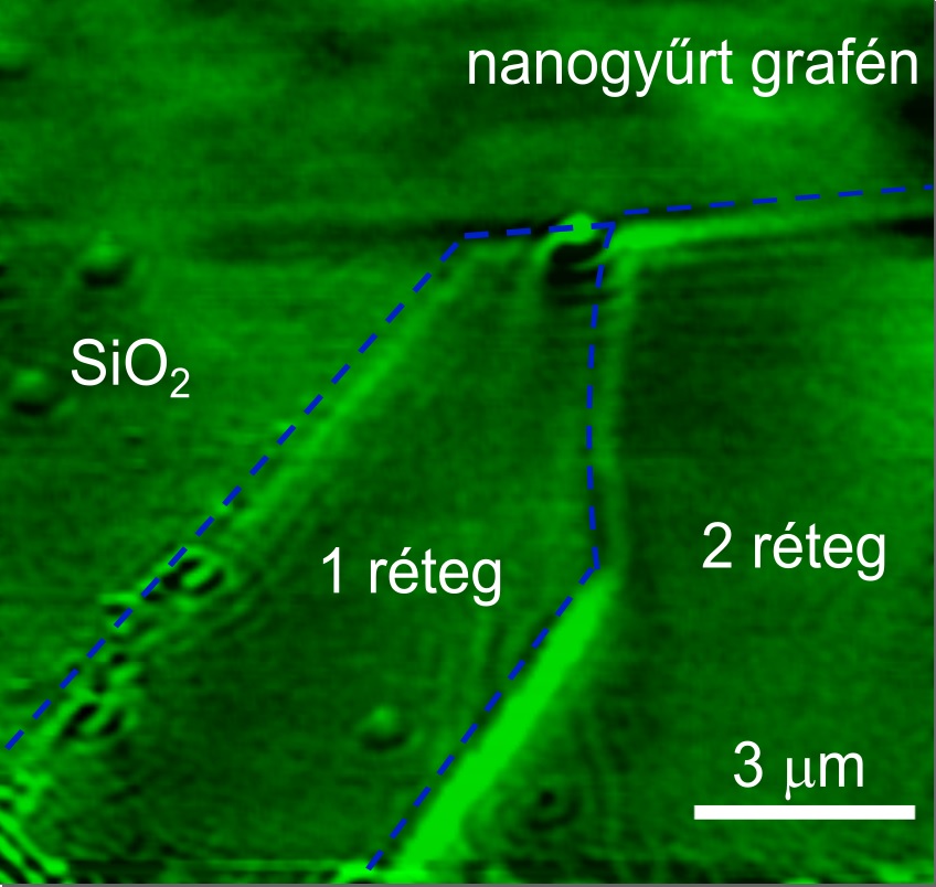
The ability of graphene to support plasmons of terahertz and infra-red frequencies has been demonstrated before. However, to reach the commercially important visible-frequency range, it has been predicted that graphene plasmons have to be confined into sub-10 nanometre size graphene structures. In order to confine graphene plasmons, first, the electrons of graphene have to be trapped into nanoscale graphene structures. The researchers of the Nanostructures Laboratory have a long-standing expertise in the area of defining such small graphene nanostructures. They have developed a scanning tunneling microscopy based nanofabrication method that even today is the most precise nanolithographic method for graphene, and is capable of defining graphene nanostructures well below 10 nm characteristic size. While this approach is efficient for confining the electrons of graphene, it did not work for plasmons. The reason is that physical edges of the small graphene nanostructures are highly detrimental for plasmons. Therefore, a novel approach was required to confine the charge carriers of graphene without the presence of edges. The researchers at Centre for Energy Research found a highly innovative solution for this problem. They have demonstrated that the electrons of graphene can also be trapped into nanoscale graphene corrugations, if they are sufficiently high. They have induced a strong structural corrugation into graphene sheets, by using a simple cyclic thermal annealing process, by subsequently heating and cooling the sample between room temperature and 400 ⁰C. Such a process exploits the difference in the thermal expansion coefficient of graphene and the substrate (SiO2), giving rise to graphene corrugations with characteristic dimensions of about 5 nm diameter, and about 1 nm height. Such structural deformations are strong enough to curve the trajectories of electrons into closed orbits, realizing their confinement into graphene nanocorrugations. The edge-free confinement of electrons, in turn enables the low-loss confinement of graphene plasmons.
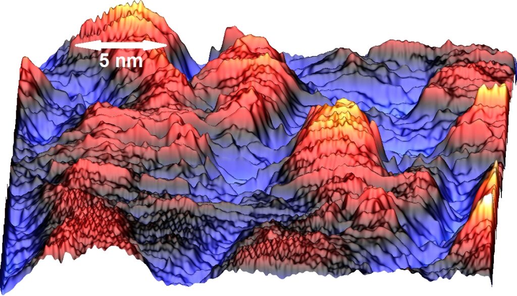
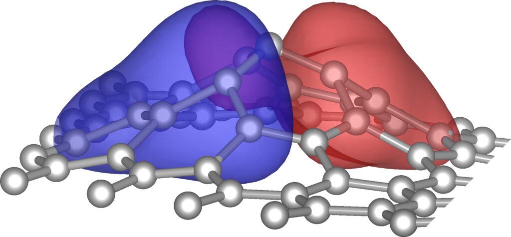
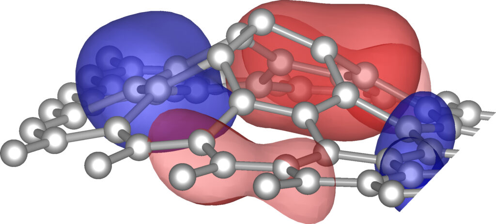
3D scanning tunneling microscopy (STM) image of nanocorrugated graphene, and the calculated charge distribution of graphene plasmons.
What are graphene plasmons good for?
Graphene plasmons are characterized by particularly strong electric near-fields, extending only a couple of tens of nanometres outwards from the surface of graphene. If a molecule approaches the graphene within such distance, it enters the strong local plasmonic fields, upon which its interaction with light can be increased millions of times. This enhanced interaction with light is of high practical significance, as it enables a much more sensitive optical detection of such molecules.
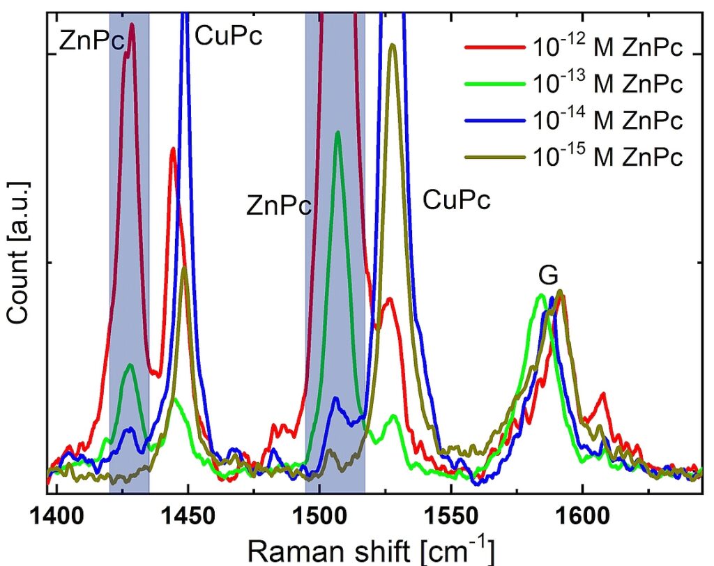
Copper- and zinc-phthalocyanine molecules detected by Raman spectroscopy at extremely low concentrations, as well as interference patterns of visible frequency graphene plasmons detected by SNOM measurements.
To demonstrate the highly sensitive optical detection with graphene plasmons, the researchers prepared highly diluted solutions of specific molecules (e.g., zinc phthalocyanine – ZnPc). They were able to detect the presence of ZnPc molecules form solutions of femtomolar concentrations. Such solutions are so dilute that a single ZnPc molecule can be found in a million times thousand millions of solution molecules. As a result, they were able to detect molecules with a thousand times improved sensitivity than previously achieved with graphene based optical sensors. Moreover, the nanocorrugated graphene based sensors have a huge practical advantage as they are much more environmentally stable than similar sensors, conventionally prepared from silver and gold nanoparticle films. While the sensitivity of noble-metal nanoparticle films can decline on the time-scale of hours due to environmental effects, nanocorrugated graphene films were shown to preserve their sensitivity for months. Due to the practical relevance of these results, the researchers have also applied for a patenting nanocorrugated graphene based sensors.
Moreover, graphene plasmons have further surprised the researchers. While in order to realize visible frequency graphene plasmons, one has to trap them into tiny graphene nanostructures, this does not mean the after they were created, they cannot break free from the traps. The researchers have demonstrated using scanning near-field optical microscopy that propagating graphene plasmons are also present in nanocorrugated graphene at visible frequencies. This is possible because graphene nanocorrugations are located in the close vicinity of each other. Consequently, the plasmons trapped into them can interact with each other, and such interaction allows them to form propagating plasmon modes. This finding is important, since propagating plasmons are envisaged for future computational and signal processing applications. Graphene is a particularly suitable material for realizing such plasmonic circuits since plasmons can propagate in graphene with relatively low loss.
Related publication:
Dobrik G., Nemes-Incze P., Majerus B., Süle P., Vancsó P., Piszter G., Menyhárd M., Kalas B., Petrik P., Henrard L., Tapasztó L.: Large-area nanoengineering of graphene corrugations for visible-frequency graphene plasmons. (2021) Nature Nanotechnology
Related patent:
Tapasztó Levente, Dobrik Gergely, Nemes-Incze Péter, Vancsó Péter: Substrate for surface enhanced Raman scattering, fabrication process, and graphene structure. P2000410